Epoxy Probe Assembly in California: Precision Testing Solutions
- Semi Probes Inc
- Jul 30, 2025
- 5 min read

Epoxy probe assembly is a specialized process that plays a vital role in industries like electronics, aerospace, and medical device manufacturing. In California, where innovation drives economic growth, epoxy probe assemblies are in high demand due to their precision and reliability.
This article explores what epoxy probe assembly entails, its importance in California’s industrial landscape, the processes involved, and why businesses in the state rely on this technology. By understanding the nuances of epoxy probe assembly, companies can make informed decisions to enhance their production capabilities and maintain a competitive edge.

What is Epoxy Probe Assembly?
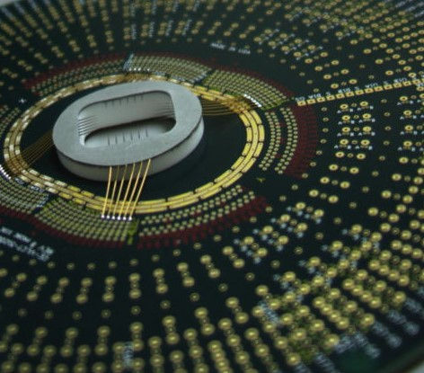
Epoxy probe assembly refers to the process of creating precise, durable components used in testing and measurement systems, particularly in the electronics and semiconductor industries. These probes are typically fine needles or pins encapsulated in epoxy resin to ensure stability, insulation, and accuracy during testing. The epoxy material provides structural support and electrical insulation, making these probes ideal for applications like integrated circuit testing, wafer probing, and other high-precision tasks.
In California, a hub for technology and innovation, epoxy probe assemblies are critical for ensuring the quality and performance of electronic components. The state’s thriving tech ecosystem, from Silicon Valley to Southern California, relies on these assemblies to maintain the high standards required for cutting-edge devices.
The assembly process begins with selecting high-quality materials, including conductive metals for the probe tips and epoxy resins that meet specific durability and thermal requirements. The probes are meticulously aligned and embedded in the epoxy, which is then cured to form a solid, reliable structure.
This precision is crucial because even a slight misalignment can lead to inaccurate test results, potentially costing companies significant time and resources. California’s manufacturers have honed this process, leveraging advanced machinery and skilled technicians to produce probes that meet the stringent demands of industries like telecommunications and medical technology.
The Role of Epoxy Probe Assembly in California’s Industries
California’s economy is heavily driven by technology, with companies in Silicon Valley, San Diego, and Los Angeles leading advancements in electronics, aerospace, and biotechnology. Epoxy probe assemblies are integral to these sectors because they enable precise testing of microchips, circuit boards, and other components.
For example, in the semiconductor industry, probes are used to test wafers before they are cut into individual chips, ensuring that only functional units move forward in production. This quality control step is essential for maintaining efficiency and reducing waste, which is particularly important in California, where environmental regulations and sustainability goals are a priority.
Beyond semiconductors, epoxy probe assemblies are used in aerospace for testing sensors and control systems, ensuring that components can withstand extreme conditions. In the medical field, these probes help verify the functionality of devices like pacemakers and diagnostic equipment.
California’s diverse industrial base benefits from the versatility of epoxy probe assemblies, which can be customized to meet specific requirements, such as varying probe lengths, tip shapes, or epoxy formulations. This adaptability makes them indispensable for companies aiming to innovate while adhering to strict quality standards.
The Manufacturing Process of Epoxy Probe Assemblies
Creating an epoxy probe assembly is a complex process that requires precision and expertise. The first step involves designing the probe to meet the specific needs of the application, such as the type of material being tested or the electrical properties required.
Engineers in California often use computer-aided design (CAD) software to create detailed blueprints, ensuring that every probe meets exact specifications. Once the design is finalized, the manufacturing process begins with selecting high-conductivity metals, such as tungsten or beryllium copper, for the probe tips. These materials are chosen for their durability and ability to maintain sharp, precise contact points.
Next, the probes are carefully positioned in a mold or fixture, and epoxy resin is poured or injected around them. The epoxy is selected based on its thermal stability, electrical insulation properties, and ability to withstand environmental factors like humidity or temperature fluctuations.
After the epoxy is applied, it undergoes a curing process, often involving heat or ultraviolet light, to harden and secure the probes in place. This step is critical, as improper curing can lead to defects like air bubbles or weak bonding, which compromise the probe’s performance. California manufacturers use state-of-the-art equipment to control curing conditions, ensuring consistent results.
Quality control is a significant part of the process. Each assembly is tested for alignment, electrical performance, and durability. In California, where industries demand high reliability, manufacturers often employ automated inspection systems and skilled technicians to verify that every probe meets industry standards. This rigorous approach ensures that epoxy probe assemblies perform reliably in demanding applications, from testing microchips in Silicon Valley to ensuring the safety of aerospace components in Los Angeles.
Why California is a Hub for Epoxy Probe Assembly
California’s status as a global leader in technology and manufacturing makes it an ideal location for epoxy probe assembly production. The state is home to some of the world’s largest tech companies, as well as numerous startups and research institutions, all of which drive demand for high-quality testing components.
Silicon Valley, in particular, is a hotspot for semiconductor manufacturing, where epoxy probe assemblies are used extensively in wafer testing. The proximity of suppliers, manufacturers, and end-users in California creates a robust ecosystem that supports rapid innovation and production.
Additionally, California’s highly skilled workforce is a key factor in its dominance in this field. The state’s universities and technical schools produce engineers and technicians trained in advanced manufacturing techniques, including those specific to epoxy probe assembly.
Companies in California also benefit from access to cutting-edge research and development facilities, allowing them to stay ahead of industry trends and develop new probe designs. Furthermore, the state’s commitment to sustainability encourages manufacturers to adopt eco-friendly practices, such as using recyclable materials or reducing waste in the epoxy curing process.
Challenges and Innovations in Epoxy Probe Assembly
While epoxy probe assembly is a well-established process, it is not without challenges. One common issue is ensuring consistent probe alignment, as even minor deviations can affect test accuracy. Manufacturers in California address this by investing in precision machinery and automation, which improve alignment accuracy and reduce human error.
Another challenge is selecting the right epoxy formulation, as different applications require specific properties, such as high thermal resistance or low dielectric constants. California’s manufacturers work closely with material scientists to develop custom epoxy blends that meet these needs.
Innovation is a driving force in California’s epoxy probe assembly industry. Recent advancements include the development of micro-probes for testing smaller, more complex chips, as well as the use of nanotechnology to enhance probe performance. Some companies are also exploring biodegradable epoxy resins to align with California’s environmental goals. These innovations ensure that California remains at the forefront of the industry, providing solutions that meet the evolving demands of technology-driven markets.
FAQs
What is the purpose of an epoxy probe assembly?
An epoxy probe assembly is used to test the functionality of electronic components, such as microchips or circuit boards, by providing precise electrical connections. The epoxy encases the probes, ensuring stability and insulation during testing.
Why is California a leader in epoxy probe assembly?
California’s leadership stems from its strong technology sector, skilled workforce, and access to advanced manufacturing facilities. The state’s proximity to major industries like semiconductors and aerospace drives demand for high-quality probe assemblies.
How long does it take to manufacture an epoxy probe assembly?
The manufacturing time varies depending on the complexity of the design and the volume required. On average, it can take anywhere from a few hours to several days, including design, assembly, curing, and quality testing.
Are epoxy probe assemblies environmentally friendly?
While traditional epoxy resins are not biodegradable, some California manufacturers are exploring eco-friendly alternatives, such as recyclable or biodegradable epoxies, to align with the state’s sustainability goals.
Can epoxy probe assemblies be customized?
Yes, epoxy probe assemblies can be tailored to meet specific requirements, including probe size, material, and epoxy properties. This customization is particularly important for industries like aerospace and medical devices.


Comments