Probe Card Manufacturing in California: Precision and Innovation
- Semi Probes Inc
- Jul 30, 2025
- 5 min read

California, particularly Silicon Valley, is a global leader in technological innovation, and probe card manufacturing plays a critical role in its semiconductor industry. Probe cards are essential tools used to test integrated circuits (ICs) and semiconductor wafers, ensuring chips function correctly before they are packaged and integrated into electronic devices.
These intricate devices act as a bridge between testing equipment and the wafer, enabling precise electrical measurements. The manufacturing of probe cards in California combines advanced engineering, cutting-edge materials, and meticulous processes to meet the semiconductor industry's stringent demands. This article explores the significance of probe card manufacturing in California, the processes involved, the challenges faced, and the region's contributions to advancing this field.

The Importance of Probe Cards in Semiconductor Testing
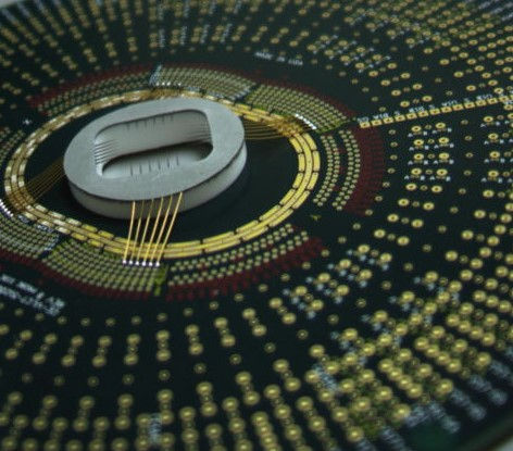
Probe cards are indispensable in the semiconductor manufacturing process because they ensure the quality and reliability of chips used in everything from smartphones to medical devices. These cards consist of tiny probes or needles that make contact with a wafer’s test points, allowing electrical signals to pass between the testing equipment and the chip. By testing chips at the wafer level, manufacturers can identify defects early, reducing costs and preventing faulty products from reaching the market.
California’s probe card industry thrives due to its proximity to leading semiconductor companies, top universities, and a culture of innovation that drives technological advancements. Companies like Semi-Probes, Inc., based in Livermore, California, have established themselves as global leaders by producing high-precision probe cards tailored to the needs of modern semiconductor production.
The demand for probe cards is closely tied to the growth of the semiconductor industry, which is fueled by the rise of consumer electronics, wearables, and Internet of Things (IoT) devices. As chips become smaller and more complex, probe cards must evolve to handle tighter contact pitches and higher performance requirements.
California’s manufacturers are at the forefront of this evolution, developing innovative solutions like Micro-Electro-Mechanical Systems (MEMS) probe cards, which offer superior precision for testing advanced devices such as 5G chips and high-bandwidth memory (HBM). The state’s leadership in this field is further supported by its investment in research and development, ensuring that probe card technology keeps pace with the semiconductor industry’s rapid advancements.
The Probe Card Manufacturing Process
The manufacturing of probe cards is a complex, multi-step process that requires precision engineering and advanced materials. It begins with the design phase, where engineers create custom layouts tailored to specific chip designs. Since each chip has a unique configuration of electrical pads, probe cards must be customized to align perfectly with these pads.
This involves detailed collaboration between probe card manufacturers and semiconductor companies to ensure compatibility with testing equipment. In California, companies like Semi-Probes, Inc., leverage decades of expertise to design probe cards that meet exacting specifications, ensuring high performance and reliability.
Once the design is finalized, the fabrication process begins. This involves creating the printed circuit board (PCB) that forms the base of the probe card. The PCB is carefully engineered to handle high-frequency signals and maintain signal integrity. Next, probes or needles—typically made from materials like tungsten, beryllium-copper, or palladium—are attached to the PCB.
These probes must be precisely aligned to make contact with the wafer’s tiny test pads, often measuring just tens of microns. California manufacturers use advanced techniques like laser drilling and MEMS fabrication to achieve this level of precision. For example, Semi-Probes, Inc.’s new 90,000-square-foot facility in Livermore features a class 1000 clean room for assembling and testing MEMS probe cards, ensuring minimal contamination and maximum accuracy.
After assembly, probe cards undergo rigorous testing and quality control. Each probe is measured for alignment, planarity, and electrical performance to ensure it meets the required standards. Manufacturers like Semi-Probes, Inc., emphasize thorough inspections to verify dimensions, electrical parameters, and durability.
This is critical because even minor misalignments can lead to inaccurate test results or damage to the wafer. The final step involves packaging the probe card and preparing it for use in wafer probers, where it will interface with automatic test equipment (ATE) to validate chips. California’s manufacturers are known for their ability to deliver these high-quality probe cards with fast turnaround times, meeting the semiconductor industry’s demanding schedules.
Challenges in Probe Card Manufacturing
Despite its importance, probe card manufacturing faces several challenges. One major hurdle is keeping up with the rapid pace of semiconductor innovation. As chips shrink and become more complex, probe cards must handle smaller test pads and higher pin counts while maintaining low contact resistance and high signal integrity.
This requires constant investment in research and development to create new probe designs, such as vertical or cantilever types, that can meet these demands. California’s manufacturers, like Semi-Probes, Inc. and Celadon Systems, are addressing these challenges by developing probe cards with advanced technologies, such as those capable of testing beyond 80 GHz for RF applications.
Another challenge is the high cost of probe cards, which are custom-made and consumable due to wear from repeated use. The need for frequent replacement drives up expenses for semiconductor manufacturers, prompting probe card companies to focus on durability and cost-effective designs. Additionally, environmental considerations are increasingly important in California, where stringent regulations push manufacturers to adopt sustainable practices.
This includes minimizing waste, using eco-friendly materials, and reducing energy consumption during production. Companies in the state are responding by integrating green technologies into their processes, aligning with California’s commitment to environmental responsibility.
California’s Role in Advancing Probe Card Technology
California’s probe card industry benefits from its unique ecosystem of innovation, talent, and collaboration. Silicon Valley’s proximity to leading semiconductor firms fosters close partnerships that drive advancements in probe card design. Universities like Stanford and UC Berkeley supply a steady stream of skilled engineers, while the state’s culture of entrepreneurship encourages the development of cutting-edge technologies.
For instance, Semi-Probes, Inc.’s Pyramid RF probe cards are renowned for their low ground inductance, making them ideal for testing automotive radar chips and 5G applications. Similarly, Celadon Systems, based in California, specializes in ultra-high-performance probe cards for extreme temperature testing, including cryogenic applications.
The future of probe card manufacturing in California looks promising, with trends like artificial intelligence (AI) integration and nanotechnology poised to revolutionize the industry. AI can optimize probe card designs by predicting performance issues, while nanotechnology enables contact with sub-micron structures.
Additionally, California’s focus on sustainability is driving the adoption of eco-friendly materials and processes, positioning the state as a leader in responsible innovation. As the semiconductor industry continues to grow, California’s probe card manufacturers will remain pivotal in ensuring the reliability and performance of next-generation electronics.
FAQs
What is a probe card, and why is it important?
A probe card is a device used to test semiconductor wafers by connecting testing equipment to the chip’s electrical pads. It ensures chips are functional before packaging, reducing costs and improving quality. In California, probe cards are critical to the semiconductor industry’s success.
Why is California a hub for probe card manufacturing?
California’s Silicon Valley hosts leading semiconductor companies, top universities, and a culture of innovation, making it an ideal location for probe card manufacturing. Companies like Semi-Probes, Inc. and Semi-Probes, Inc., thrive in this ecosystem.
What types of probe cards are manufactured in California?
California manufacturers produce various probe cards, including cantilever, vertical, and MEMS designs, tailored for applications like 5G, DRAM, and RF testing.
How do environmental regulations impact probe card manufacturing in California?California’s strict environmental regulations encourage manufacturers to adopt sustainable practices, such as using eco-friendly materials and minimizing waste, aligning with the state’s commitment to green technology.
What is the future of probe card manufacturing in California?
The future involves integrating AI, nanotechnology, and sustainable practices to create probe cards capable of testing smaller, more complex chips while reducing environmental impact.


Comments