Palladium Probes Material in Santa Clara: Applications & Innovations
- Semi Probes Inc
- Jul 30, 2025
- 5 min read

Palladium, a rare and lustrous silvery-white metal, plays a significant role in various high-tech industries, particularly in Santa Clara, California, a hub for technological innovation. Known for its exceptional properties like corrosion resistance, high conductivity, and catalytic capabilities, palladium is a critical material in manufacturing advanced probes used in semiconductor testing, medical devices, and other precision applications.
This article explores the significance of palladium probes material in Santa Clara, delving into its properties, applications, manufacturing processes, and the local industry’s role in advancing this technology. By understanding palladium’s unique characteristics and its relevance in Santa Clara’s tech ecosystem, we can appreciate its impact on modern innovation.

Why Palladium is Ideal for Probes
Palladium’s appeal as a material for probes stems from its remarkable physical and chemical properties. It belongs to the platinum group metals, which are known for their durability and resistance to tarnishing. Palladium is particularly valued for its ability to withstand harsh environments, making it suitable for applications requiring long-term reliability. In Santa Clara, where semiconductor manufacturing and testing are central to the economy, palladium’s high electrical conductivity ensures precise signal transmission, critical for testing integrated circuits and microchips.
Its resistance to oxidation means probes made from palladium maintain their performance over time, even when exposed to air or other reactive conditions. Additionally, palladium’s ductility allows it to be shaped into fine, precise probe tips, essential for contacting tiny components on semiconductor wafers without causing damage. These qualities make palladium a preferred choice for manufacturers in Santa Clara’s competitive tech landscape.
Applications of Palladium Probes in Santa Clara
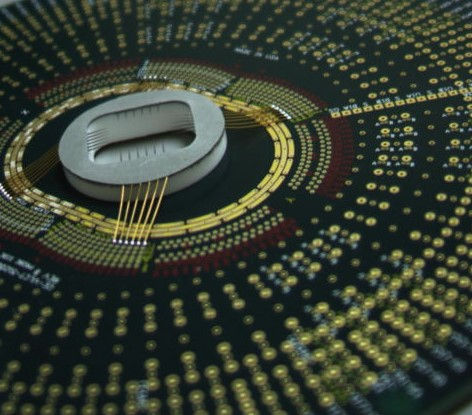
Santa Clara, often referred to as the heart of Silicon Valley, hosts numerous companies specializing in semiconductor production and testing. Palladium probes are integral to the wafer testing process, where they make contact with microchip circuits to evaluate their performance before they are packaged into final products. These probes ensure accurate electrical testing, identifying defects that could affect device functionality.
Beyond semiconductors, palladium probes are used in medical applications, such as in diagnostic equipment where precision and biocompatibility are crucial. For instance, palladium’s non-reactive nature makes it suitable for probes in devices that interact with biological tissues.
In Santa Clara, companies leverage palladium’s versatility to innovate in fields like aerospace and telecommunications, where probes are used for quality control and signal integrity testing. The local industry’s focus on cutting-edge technology amplifies the demand for high-quality palladium probes, driving advancements in material science and manufacturing techniques.
Manufacturing Palladium Probes in Santa Clara
The production of palladium probes in Santa Clara involves sophisticated processes to ensure precision and reliability. Manufacturers start with high-purity palladium, often sourced from mining operations or recycled from catalytic converters and electronic scrap. The metal is refined to remove impurities, ensuring optimal performance for probe applications. Advanced techniques like electron-beam-induced deposition (EBID) and laser ablation are used to create palladium nanostructures, such as nanowires and thin films, which form the basis of probe tips.
These methods allow for precise control over the probe’s geometry, ensuring they can contact microscopic components without causing damage. In Santa Clara, companies like Semi-Probes Incorporated utilize vacuum evaporation and other deposition techniques to coat substrates with palladium, enhancing probe durability and conductivity.
These manufacturing processes are supported by Santa Clara’s robust infrastructure, including access to cutting-edge equipment and skilled engineers, making the region a leader in probe production.
Palladium’s Role in Santa Clara’s Tech Ecosystem
Santa Clara’s position as a global technology hub amplifies the importance of palladium probes in its economy. The region is home to major semiconductor companies, research institutions, and material science innovators, all of which rely on high-performance materials like palladium. Local firms collaborate with universities and research centers to explore new applications for palladium, such as in hydrogen sensing and electrocatalysis.
For example, palladium’s ability to absorb large amounts of hydrogen makes it valuable for developing sensors used in clean energy technologies, an area of growing interest in Santa Clara. Additionally, the region’s focus on sustainability has led to innovations in recycling palladium from electronic waste, reducing reliance on mined resources and aligning with environmental goals. This synergy between industry, academia, and sustainability initiatives positions Santa Clara as a key player in advancing palladium-based technologies.
Challenges and Innovations in Palladium Probe Technology
Despite its advantages, working with palladium presents challenges, particularly in terms of cost and availability. Palladium is a precious metal, and its price has risen significantly in recent years due to supply constraints and increasing demand. In Santa Clara, manufacturers address this by developing cost-effective alloys, combining palladium with other metals like nickel or copper to maintain performance while reducing costs.
Another challenge is ensuring the probes’ longevity under high-stress conditions, such as repeated contact with semiconductor wafers. Innovations in nanotechnology, such as palladium-based nanocatalysts supported on zinc ferrite, have improved probe durability and performance in demanding applications.
Santa Clara’s tech community is also exploring machine learning and high-throughput techniques to optimize palladium probe designs, accelerating the development of next-generation materials. These advancements ensure that palladium probes remain competitive in the fast-evolving tech landscape.
The Future of Palladium Probes in Santa Clara
Looking ahead, the role of palladium probes in Santa Clara is poised to grow as technology continues to advance. The rise of 5G, artificial intelligence, and electric vehicles increases the demand for high-performance semiconductors, driving the need for reliable testing probes. Palladium’s unique properties, such as its catalytic activity and hydrogen absorption capacity, make it a candidate for emerging applications like hydrogen fuel cells and advanced sensors.
Santa Clara’s investment in research and development, supported by institutions like Santa Clara University and local industry leaders, fosters innovation in palladium-based technologies. Additionally, efforts to improve palladium recycling and develop sustainable sourcing methods will help address supply challenges, ensuring the material’s availability for future applications. As Santa Clara continues to lead in technology, palladium probes will remain a cornerstone of its innovation ecosystem.
FAQs
What makes palladium a good material for probes in Santa Clara’s industries?
Palladium’s high electrical conductivity, corrosion resistance, and ductility make it ideal for probes used in semiconductor testing and medical devices. Its ability to maintain performance in harsh conditions ensures reliability in Santa Clara’s high-tech applications.
How are palladium probes manufactured in Santa Clara?
Manufacturers use advanced techniques like electron-beam-induced deposition and laser ablation to create palladium nanostructures. These methods allow for precise shaping of probe tips, which are coated onto substrates using vacuum evaporation to enhance durability.
Why is Santa Clara a hub for palladium probe production?
Santa Clara’s role as a technology hub, with access to skilled engineers, cutting-edge equipment, and research institutions, makes it an ideal location for producing high-quality palladium probes for semiconductor and other industries.
What are the challenges of using palladium in probes?
The high cost and limited supply of palladium pose challenges. Santa Clara’s manufacturers address this by developing palladium alloys and improving recycling methods to reduce costs and environmental impact.
What is the future of palladium probes in Santa Clara?
With the growth of 5G, AI, and clean energy technologies, palladium probes will see increased demand. Innovations in nanotechnology and sustainable sourcing will ensure their continued relevance in Santa Clara’s tech ecosystem.


Comments